How to draw a CMOS NAND gate in Tanner EDA
November 4, 2023 2025-12-02 5:05How to draw a CMOS NAND gate in Tanner EDA
How to draw a CMOS NAND gate in Tanner EDA
What is a NAND gate?
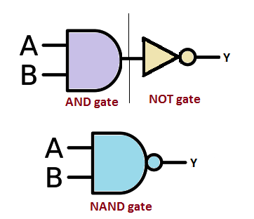
The NAND gate or “NotAND” gate is the combination of two basic logic gates, the AND gate and the NOT gate connected in series. The NAND gate and NOR gate can be called the universal gates since the combination of these gates can be used to realize any of the basic operations.
The output of a NAND gate is high when one of the inputs are low or if both the inputs are low. In other words, the output of the NAND gate is always low when both the inputs are high. The logic NAND function is given by the Boolean expression.
![]()
Where A, B are the inputs and Y is the output.
Symbol and Truth Table
Symbol


Symbol
|
A |
B |
Y |
|
0 |
0 |
1 |
|
0 |
1 |
1 |
|
1 |
0 |
1 |
|
1 |
1 |
0 |
CMOS NAND gate

Working principle of CMOS NAND gate
Case 1: A=B=0 Both the NMOS are in OFF state condition and PMOS are in ON state condition. Therefore the output is connected to VDD and HIGH logic is present at the output terminal.
Case2: A=0 and B=1, the upper NMOS are in OFF state and lower NMOS in ON condition. Left PMOS are in ON state and right PMOS in OFF condition. Therefore the output is connected to VDD and HIGH logic is maintained at the output terminal.
Case:3 When A=1 and B=0, upper NMOS are in ON and lower NMOS in OFF condition. Left PMOS are in OFF and right PMOS in ON condition. Therefore the output is connected to VDD and HIGH logic is maintained at the output terminal.
Case:4 When A=B=1,both the NMOS are in ON condition and PMOS are in OFF condition. Therefore the output is connected to GND and LOW logic is present at the output terminal.
Output waveform
